7.2. Components of Hardware Accelerators
A hardware accelerator typically comprises multiple on-chip caches and various types of arithmetic units. In this section, we’ll examine the fundamental components of hardware accelerators, using the Nvidia Volta GPU architecture as a representative example.
7.2.1. Architecture of Accelerators
Contemporary graphics processing units (GPUs) offer remarkable computing speed, ample memory storage, and impressive I/O bandwidth. A top-tier GPU frequently surpasses a conventional CPU by housing double the number of transistors, boasting a memory capacity of 16 GB or greater, and operating at frequencies reaching up to 1 GHz. The architecture of a GPU comprises streaming processors and a memory system, interconnected through an on-chip network. These components can be expanded independently, allowing for customized configurations tailored to the target market of the GPU.
Figure :numref:ch06/ch06-gv100 illustrates the architecture of the
Volta GV100 . This architecture has:
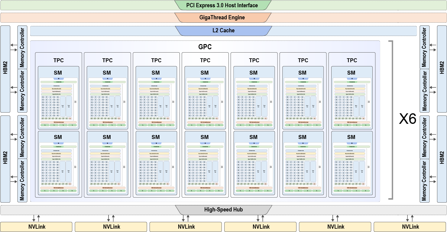
Fig. 7.2.1 Volta GV100
6 GPU processing clusters (GPCs), each containing:
7 texture processing clusters (TPCs), each containing two streaming multiprocessors (SMs).
14 SMs.
84 SMs, each containing:
64 32-bit floating-point arithmetic units
64 32-bit integer arithmetic units
32 64-bit floating-point arithmetic units
8 Tensor Cores
4 texture units
8 512-bit memory controllers.
As shown in Figure :numref:ch06/ch06-gv100, a GV100 GPU contains
84 SMs (Streaming Multiprocessors), 5376 32-bit floating-point
arithmetic units, 5376 32-bit integer arithmetic units, 2688 64-bit
floating-point arithmetic units, 672 Tensor Cores, and 336 texture
units. A pair of memory controllers controls an HBM2 DRAM stack.
Different vendors may use different configurations (e.g., Tesla V100 has
80 SMs).
7.2.2. Memory Units
The memory units of a hardware accelerator resemble a CPU’s memory controller. However, they encounter a bottleneck when retrieving data from the computer system’s DRAM, as it is slower compared to the processor’s computational speed. Without a cache for quick access, the DRAM bandwidth becomes inadequate to handle all transactions of the accelerator. Consequently, if program instructions or data cannot be swiftly retrieved from the DRAM, the accelerator’s efficiency diminishes due to prolonged idle time. To tackle this DRAM bandwidth issue, GPUs employ a hierarchical design of memory units. Each type of memory unit offers its own maximum bandwidth and latency. To fully exploit the computing power and enhance processing speed, programmers must select from the available memory units and optimize memory utilization based on varying access speeds.
Register file: Registers serve as the swiftest on-chip memories. In contrast to CPUs, each SM in a GPU possesses tens of thousands of registers. Nevertheless, excessively utilizing registers for every thread can result in a reduced number of thread blocks that can be scheduled within the SM, leading to fewer executable threads. This underutilization of hardware capabilities hampers performance considerably. Consequently, programmers must judiciously determine the appropriate number of registers to employ, taking into account the algorithm’s demands.
Shared memory: The shared memory is a level-1 cache that is user-controllable. Each SM features a 128 KB level-1 cache, with the ability for programmers to manage up to 96 KB as shared memory. The shared memory offers a low access latency, requiring only a few dozen clock cycles, and boasts an impressive bandwidth of up to 1.5 TB/s. This bandwidth is significantly higher than the peak bandwidth of the global memory, which stands at 900 GB/s. In high-performance computing (HPC) scenarios, engineers must possess a thorough understanding of how to leverage shared memory effectively.
Global memory: Both GPUs and CPUs are capable of reading from and writing to global memory. Global memory is visible and accessible by all threads on a GPU, whereas other devices like CPUs need to traverse buses like PCIe and NV-Link to access the global memory. The global memory represents the largest memory space available in a GPU, with capacities reaching over 80 GB. However, it also exhibits the longest memory latency, with a load/store latency that can extend to hundreds of clock cycles.
Constant memory: The constant memory is a virtual address space in the global memory and does not occupy a physical memory block. It serves as a high-speed memory, specifically designed for rapid caching and efficient broadcasting of a single value to all threads within a warp.
Texture memory: Texture memory is a specialized form of global memory that is accessed through a dedicated texture cache to enhance performance. In earlier GPUs without caches, the texture memory on each SM served as the sole cache for data. However, the introduction of level-1 and level-2 caches in modern GPUs has rendered the texture memory’s role as a cache obsolete. The texture memory proves most beneficial in enabling GPUs to execute hardware-accelerated operations while accessing memory units. For instance, it allows arrays to be accessed using normalized addresses, and the retrieved data can be automatically interpolated by the hardware. Additionally, the texture memory supports both hardware-accelerated bilinear and trilinear interpolation for 2D and 3D arrays, respectively. Moreover, the texture memory facilitates automatic handling of boundary conditions based on array indices. This means that operations on array elements can be carried out without explicit consideration of boundary situations, thus avoiding the need for extra conditional branches in a thread.
7.2.3. Compute Units
Hardware accelerators offer a variety of compute units to efficiently
handle various neural networks.
Figure :numref:ch06/ch06-compute-unit demonstrates how different
layers of neural networks select appropriate compute units.
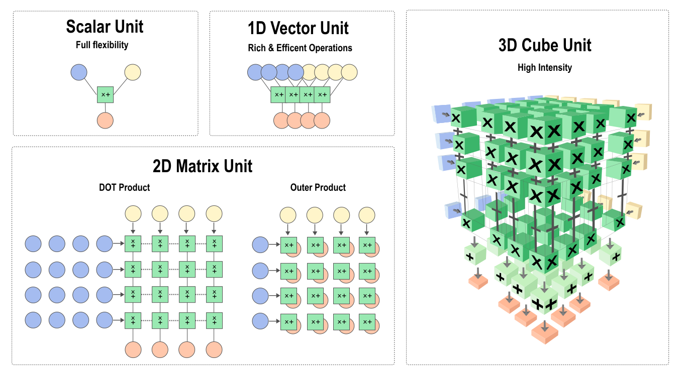
Fig. 7.2.2 Computeunits
Scalar Unit: calculates one scalar element at a time, similar to the standard reduced instruction set computer (RISC).
1D Vector Unit: computes multiple elements at a time, similar to the SIMD used in traditional CPU and GPU architectures. It has been widely used in HPC and signal processing.
2D Matrix Unit: computes the inner product of a matrix and a vector or the outer product of a vector within one operation. It reuses data to reduce communication costs and memory footprint, which achieves the performance of matrix multiplication.
3D Cube Unit: completes matrix multiplication within one operation. Specially designed for neural network applications, it can reuse data to compensate for the gap between the data communication bandwidth and computing.
The compute units on a GPU mostly include Scalar Units and 3D Cube
Units. As shown in Figure :numref:ch06/ch06-SM, each SM has 64
32-bit floating-point arithmetic units, 64 32-bit integer arithmetic
units, 32 64-bit floating-point arithmetic units, which are Scalar
Units, and 8 Tensor Cores, which are 3D Cube Units specially designed
for neural network applications.
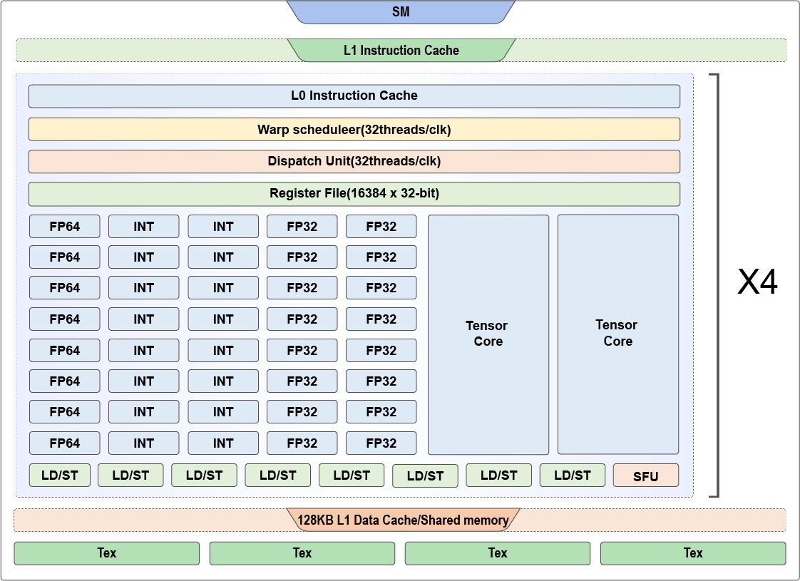
Fig. 7.2.3 Volta GV100 SM
A Tensor Core is capable of performing one \(4\times4\) matrix
multiply-accumulate operation per clock cycle, as shown in
Figure :numref:ch06/ch06-tensorcore.
D = A * B + C
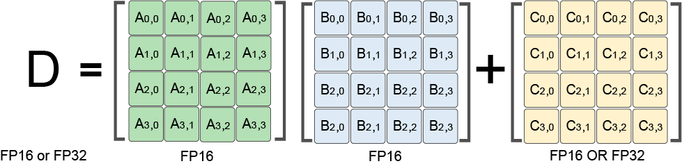
Fig. 7.2.4 Tensor Core’s \(4\times4\) matrix multiply-accumulateoperation
\(\bf{A}\), \(\bf{B}\), \(\bf{C}\), and \(\bf{D}\) are \(4\times4\) matrices. Input matrices \(\bf{A}\) and \(\bf{B}\) are FP16 matrices, and accumulation matrices \(\bf{C}\) and \(\bf{D}\) can be either FP16 or FP32 matrices. Tesla V100’s Tensor Cores are programmable matrix multiply-accumulate units that can deliver up to 125 Tensor Tera Floating-point Operations Per Second (TFLOPS) for training and inference applications, resulting in a ten-fold increase in computing speed when compared with common FP32 compute units.
7.2.4. Domain Specific Architecture
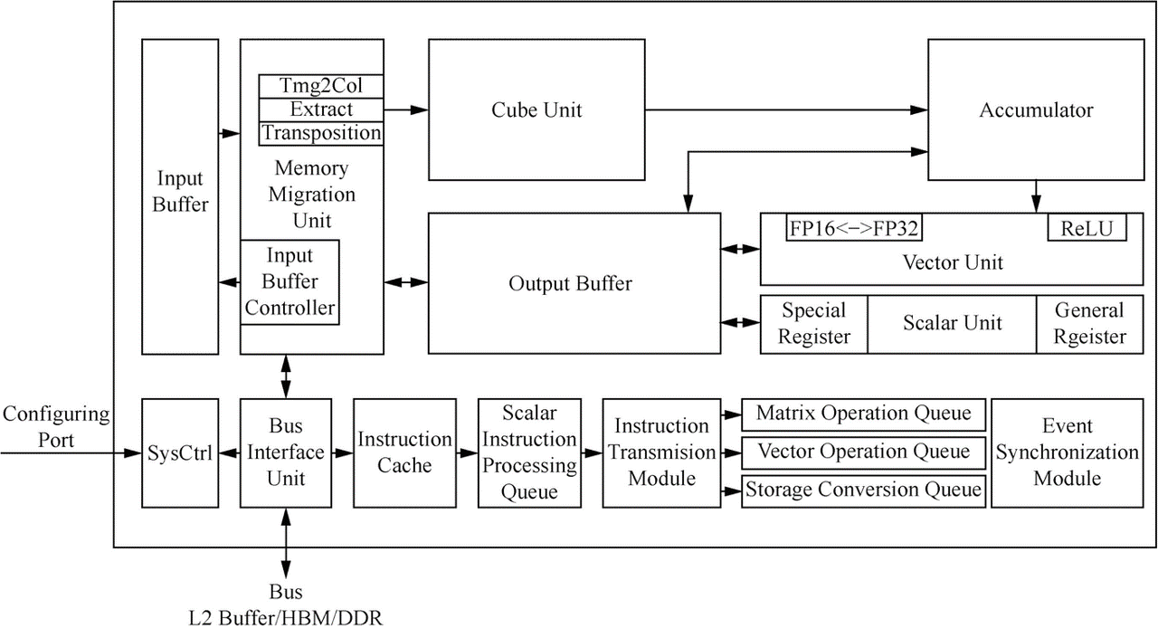
Fig. 7.2.5 Da Vinciarchitecture
Domain Specific Architecture (DSA) has been an area of interest in meeting the fast-growing demand for computing power by deep neural networks. As a typical DSA design targeting image, video, voice, and text processing, neural network processing units (or namely deep learning hardware accelerators) are system-on-chips (SoCs) containing special compute units, large memory units, and the corresponding control units. A neural processing unit, for example, Ascend chip, typically consists of a control CPU, a number of AI computing engines, multi-level on-chip caches or buffers, and the digital vision pre-processing (DVPP) module.
The computing core of AI chips is composed of AI Core, which is
responsible for executing scalar- and tensor-based arithmetic-intensive
computing. Consider the Ascend chip as an example. Its AI Core adopts
the Da Vinci architecture.
Figure :numref:ch06/ch06-davinci_architecture shows the
architecture of an AI Core, which can be regarded as a simplified
version of modern microprocessor architecture from the control
perspective. It includes three types of basic computing units: Cube
Unit, Vector Unit, and Scalar Unit. These units are used to compute on
tensors, vectors, and scalars, respectively, in three independent
pipelines centrally scheduled through the system software to coordinate
with each other for higher efficiency. Similar to GPU designs, the Cube
Unit functions as the computational core of the AI Core and delivers
parallel acceleration for matrix multiply-accumulate operations.
Specifically, it can multiply two \(16\times16\) matrices in a
single instruction — equivalent to completing 4096
(=:math:16times16times16) multiply-accumulate operations within an
extremely short time — with precision comparable to FP16 operations.